


Ushering in a new era of collaborative innovation, top American semiconductor companies have announced some major investments towards accelerating India’s Semiconductor Mission (ISM) during Prime Minister Narendra Modi’s visit to the United States.
Strengthening of semiconductor supply chains has been listed as the top item by the White House as it unveiled the ‘technology partnership for the future’ between the two countries following the talks between PM Modi and US President Joe Biden in Washington on Thursday.
It takes forward the goals outlined in the Memorandum of Understanding (MoU) signed by US Secretary of Commerce Gina Raimondo and India’s Minister of Commerce and Industry Piyush Goyal on ‘Semiconductor Supply Chain and Innovation Partnership’ during the India-US Commercial Dialogue held in New Delhi on March 10.
The agreement seeks to establish a collaborative mechanism between the two governments on semiconductor supply chain resiliency and diversification in view of the US’s CHIPS and Science Act and India’s Semiconductor Mission.
Semiconductors are an essential component of electronic devices, enabling advances in communications, computing, healthcare, military systems, transportation, clean energy, and countless other applications.
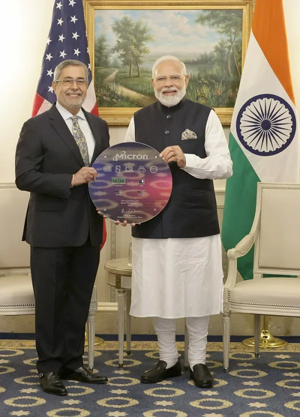
Earlier today, Micron Technology, one of the world’s largest chip makers, announced that it will invest more than $800 million towards building a new $2.75 billion semiconductor assembly and test facility in Gujarat.
The construction of the new unit is expected to begin this year with the first phase, which will include 500,000 square feet of planned cleanroom space, slated to become operational in late 2024. Micron said that it will ramp capacity gradually over time in line with global demand trends and expects Phase 2 of the project, which would include the construction of a facility similar in scale to Phase 1, to start towards the second half of the decade.
The new facility will enable assembly and test manufacturing for both Dynamic Random Access Memory (DRAM) and NAND products and address demand from domestic and international markets.
Micron will receive 50% financial support for the total project cost from the Indian government and incentives representing 20% of the total project cost from the state of Gujarat. The combined investment by Micron and the two government entities over the course of both phases will be up to $2.75 billion.
“We are excited about the steps India is taking to develop the local semiconductor ecosystem… Our new assembly and test location in India will enable Micron to expand our global manufacturing base and better serve our customers in India and around the world,” said Micron President and CEO Sanjay Mehrotra who met PM Modi in Washington on June 21.
Micron’s new facility will focus on transforming wafers into ball grid array (BGA) integrated circuit packages, memory modules and solid-state drives.
“Micron’s investment to set up assembly and test manufacturing in India will fundamentally transform India’s semiconductor landscape and generate tens of thousands of high-tech and construction jobs,” said Minister for Railways, Communications, Electronics and IT Ashwini Vaishnaw.
‘I had an excellent meeting with PM @narendramodi. I am very impressed with the vision PM Modi has for India and the advances that India is making’, says @MicronTech CEO, Sanjay Mehrotra@PMOIndia @MicronCEO #IndiaUSAPartnership #USWelcomesModi https://t.co/ai8sWG80cb pic.twitter.com/BEgvy23hIF
— DD News (@DDNewslive) June 21, 2023
Based in California’s Silicon Valley, Applied Materials – a leader in materials engineering solutions used to produce virtually every new chip and advanced display in the world – has also announced its intention to build a collaborative engineering centre in Bengaluru.
The centre will be designed to bring together applied engineers, leading global and domestic suppliers, and top research and academic institutions, enabling them to collaborate in one location with a common goal of accelerating the development of semiconductor equipment sub-systems and components.
It will also aim to serve as a catalyst for the training and development of future semiconductor industry talent, as well as open up new opportunities for India to play an expanded role in the global chip ecosystem.
President & CEO of @Applied4Tech, Mr. Gary E. Dickerson, had a meeting with PM @narendramodi in Washington DC. They discussed ways to strengthen the semiconductor ecosystem in India. pic.twitter.com/y34TIcwtuh
— PMO India (@PMOIndia) June 22, 2023
“Applied is excited to build upon our 20 years of success in India by creating a facility where the country’s top engineers, suppliers and researchers can work side-by-side to develop new innovations,” said Prabu Raja, President of the Semiconductor Products Group at Applied Materials.
Applied intends to make a gross investment of $400 million over four years to establish the new centre in India. In its first five years of operation, it is expected to support more than $2 billion of planned investments and create at least 500 new advanced engineering jobs along with potentially another 2,500 jobs in the manufacturing ecosystem.
“We envision Applied’s strong base of engineering talent collaborating more deeply with domestic and global companies operating in India to strengthen the foundational equipment supply chain serving the global semiconductor manufacturing industry,” added Raja.
Dr. Prabu Raja, Global Head of Semiconductor Business, Applied Materials India Pvt. Ltd @Applied4Tech called on me at my office @GoI_MeitY today. pic.twitter.com/HCrcvm1kQI
— Rajeev Chandrasekhar 🇮🇳 (@Rajeev_GoI) June 14, 2023
Similarly, Fremont-based Lam Research Corporation, a global supplier of innovative wafer fabrication equipment and services to the semiconductor industry, announced on Friday that it will help train the next generation of semiconductor engineers in India.
The programme is targeted to educate up to 60,000 Indian engineers in nanotechnologies over a 10-year period, in support of India’s semiconductor education and workforce development goals.
Lam believes that its Semiverse Solutions portfolio is a game-changer that provides a foundation to create a virtual semiconductor innovation universe at a time when the semiconductor industry faces a major talent shortage to meet anticipated future demand.
“The role semiconductors play in enabling everything from artificial intelligence to electric vehicles is fueling a greater need for nanotechnology expertise around the world. We look forward to working with the government of India in support of their goal to fast-track the education and training of the next generation of semiconductor engineers,” said Lam Research President and CEO Tim Archer.
Today at the White House, we announced a proposal to train up to 60,000 engineering students in India using SEMulator3D®, our Semiverse™ Solutions virtual fabrication platform. Learn more about Semiverse Solutions: https://t.co/5HVJbh9SSZ pic.twitter.com/ky7RN1p0FY
— Lam Research (@LamResearch) June 22, 2023
In addition, the US Semiconductor Industry Association and India Electronics Semiconductor Association (IESA) have also released an interim readiness assessment to identify near-term industry opportunities and facilitate the long-term strategic development of complementary semiconductor ecosystems.
In India, technology is not only about innovation but also about inclusion. pic.twitter.com/QFCKOeULXp
— Narendra Modi (@narendramodi) June 23, 2023
India remains focused on its important objective of building the overall semiconductor outlook and ensuring that it in turn catalyses the country’s rapidly expanding electronics manufacturing and innovation ecosystem.
The government led by PM Modi has already approved the Semicon India programme with a total outlay of Rs 76,000 crore for the development of the semiconductor and display manufacturing ecosystem in the country.
#WATCH | Union Minister Rajeev Chandrasekhar speaks on the PM’s invitation to American chip maker Micron Technology to boost semiconductor manufacturing in India. pic.twitter.com/IQMgbKKlvJ
— ANI (@ANI) June 23, 2023
The programme has further been modified in view of the aggressive incentives offered by countries already having established semiconductor ecosystems and a limited number of companies owning advanced node technologies.